Introduction to Semiconductor Materials
Scientists are working hard to discover new semiconductor materials that could improve the efficiency of solar cells and other electronics. However, the pace of innovation is slow due to the time it takes to manually measure important material properties. A new autonomous robotic system developed by MIT researchers could change this.
How the Robotic System Works
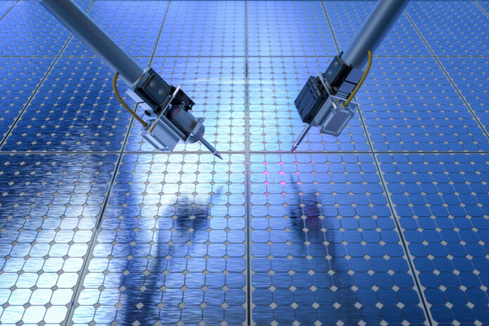
The system uses a robotic probe to measure an important electrical property known as photoconductance, which is how electrically responsive a material is to light. The researchers have incorporated materials-science-domain knowledge from human experts into the machine-learning model that guides the robot’s decision-making. This enables the robot to identify the best places to contact a material with the probe to gain the most information about its photoconductance.
Key Features of the System
A specialized planning procedure finds the fastest way to move between contact points, making the process more efficient. During a 24-hour test, the fully autonomous robotic probe took more than 125 unique measurements per hour, with more precision and reliability than other artificial intelligence-based methods.
Potential Impact
By increasing the speed at which scientists can characterize important properties of new semiconductor materials, this method could lead to the development of solar panels that produce more electricity. According to Tonio Buonassisi, professor of mechanical engineering, "I find this paper to be incredibly exciting because it provides a pathway for autonomous, contact-based characterization methods."
Making Contact with Materials
Since 2018, researchers in Buonassisi’s laboratory have been working towards a fully autonomous materials discovery laboratory. They have focused on discovering new perovskites, a class of semiconductor materials used in photovoltaics like solar panels. To characterize the photoconductance of these materials, a probe must be placed onto the material, and a light must be shone on it to measure the electrical response.
The Autonomous System in Action
The robotic system uses its onboard camera to take an image of a slide with perovskite material printed on it. Then, it uses computer vision to cut that image into segments, which are fed into a neural network model that incorporates domain expertise from chemists and materials scientists. The model determines the optimal points for the probe to contact based on the shape of the sample and its material composition.
Results and Future Directions
The researchers tested each component of the system and found that the neural network model found better contact points with less computation time than other AI-based methods. The path planning algorithm consistently found shorter path plans than other methods. When they put all the pieces together to conduct a 24-hour fully autonomous experiment, the robotic system conducted more than 3,000 unique photoconductance measurements at a rate exceeding 125 per hour.
Conclusion
The autonomous robotic system developed by MIT researchers has the potential to revolutionize the discovery of new semiconductor materials. By increasing the speed and precision of material characterization, this system could lead to the development of more efficient solar panels and other electronics. As the researchers continue to build on this system, they are one step closer to creating a fully autonomous lab for materials discovery, which could have a significant impact on the field of sustainability and beyond.

